

USE 6800 hardware
The computer is built out of discrete cards that are pushed into a backplane. All cards have the same two connectors that plug into the backplane, but so far I'm unsure if all connectors are wired the same, or if the cards have to sit in a specific slot. The floppy drives are also connected to the backplane with the same two connectors, and at a glance it looked like they were more or less connected straight through with no logic between the floppy and the floppy controller. Investigations will have to be made...
CPU card P/N ROF 137 3204
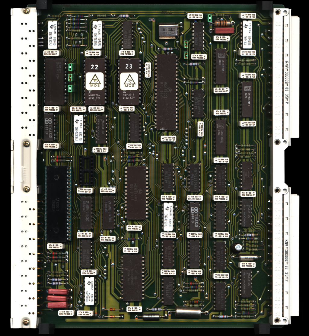
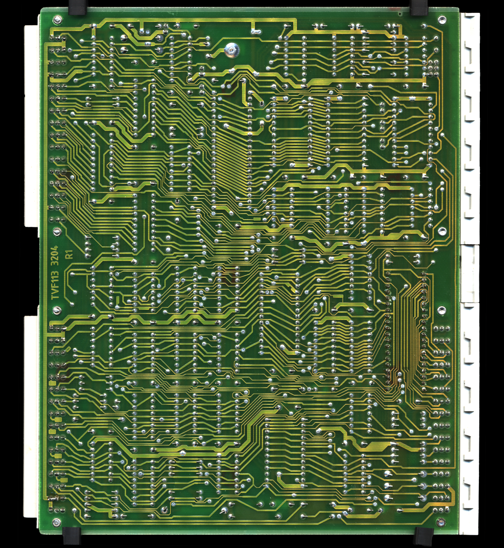
Apart from the Motorola MC68B00S CPU, there are quite a few other ICs on the card; a Motorola MC68B40S programmable timer module, a Motorola MC68B50S ACIA, two Fujitsu MBM2716 EPROMs, a Thomson EF6821P PIA, a Fujitsu MB472 (see the identification lead below), and a bunch of glue logic. Fun fact: The only card (not counting the simple power distribution card and the peripheral display/keypad) without any bodge wires.
The MB472 has finally turned up a useful lead: a Japanese photographed component collection identifies it as a priority interrupt controller compatible with Motorola's MC6828. I haven't found a Fujitsu datasheet to confirm that, so for now it's a lead rather than a confirmed replacement part. The Motorola MC6828/MC8507 datasheet describes a 24-pin device with eight latched interrupt inputs, priority masking, and logic that changes the interrupt-vector addresses seen by the ROM. That would be a useful thing to have on a machine with this many peripherals, and the package matches the MB472 in the scans. Checking the actual pin connections against that datasheet should tell us rather more than the marking alone.
The CPU card (albeit not this one) was sitting in slot 1 of the backplane when I got the machine. We'll see if that's correct, but it seems likely.
CPU card P/N N/A
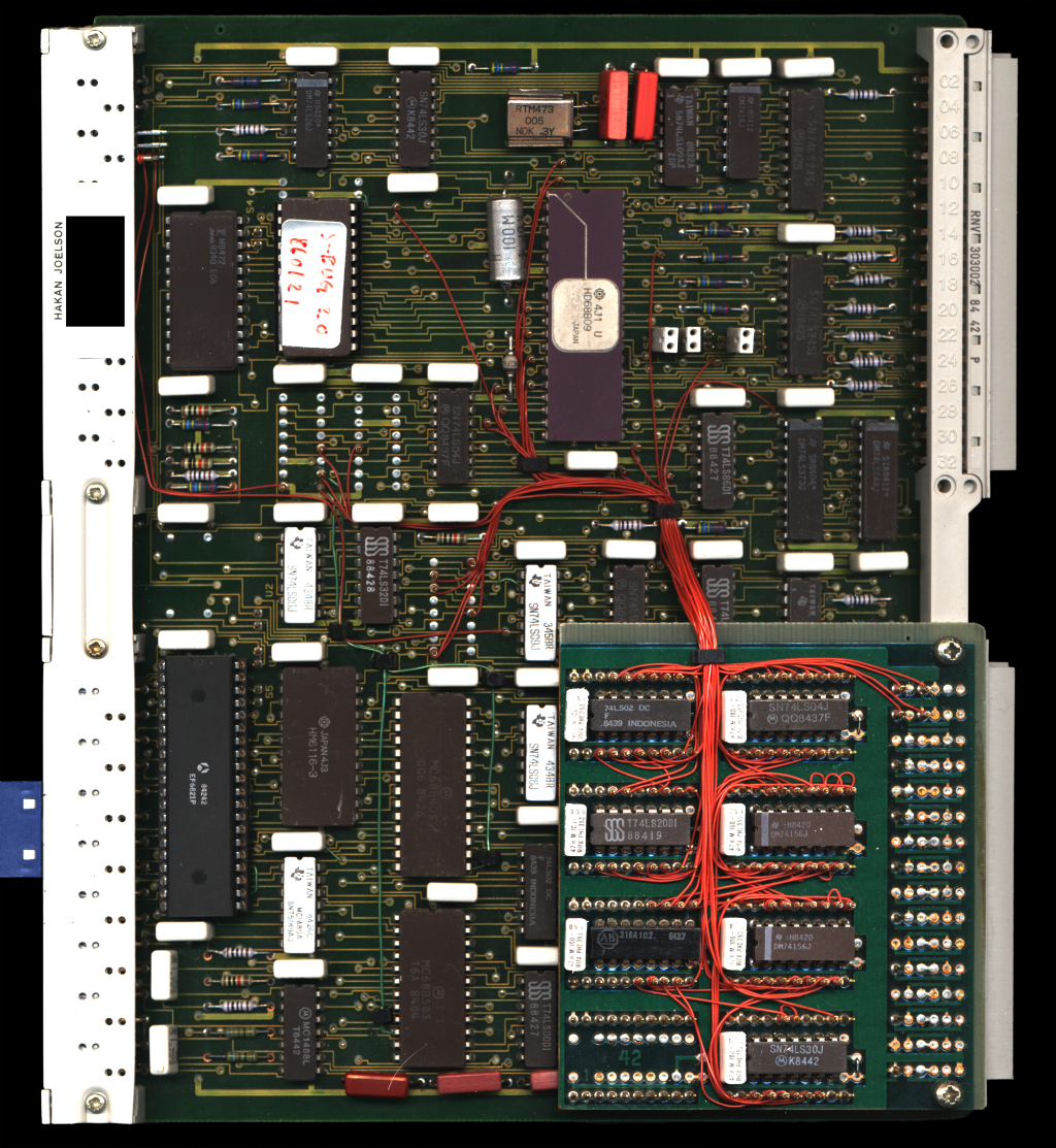
The daughter board is mostly small logic ICs, including a 74LS02, 74LS04, 74LS20 and a pair of 74156s, with an impressively organised bundle of red wires running back to the CPU area, logic sockets and other points on the main PCB. There are even little ties keeping the bundle together. Compared with the odd yellow bodge wire on the other cards, this looks like a fairly deliberate conversion job. Exactly how much of it is address decoding, interrupt handling or adapting the CPU signals will have to be worked out by following the connections; the part numbers alone don't tell us which problem each gate was put there to solve.
There is also a Hitachi HM6116-3 SRAM on the CPU card itself, adding 2 kB of physically fitted memory alongside the separate RAM card. That doesn't automatically mean 2 kB more usable memory, as it depends on where it's mapped. The EPROM label appears to read "J-BUG 2.0", with "860121" underneath, although the first letter isn't entirely clear in the scan. Tempting clues, but neither the exact monitor nor the meaning of the number should be taken for granted before the ROM has been dumped. The MC68B40S timer, MC68B50S ACIA and EF6821P PIA are still present as well, so the upgrade seems to have retained quite a lot of the original card's peripheral hardware.
This was the CPU card that was installed when I got the machine.
RAM card P/N ROF 137 3201
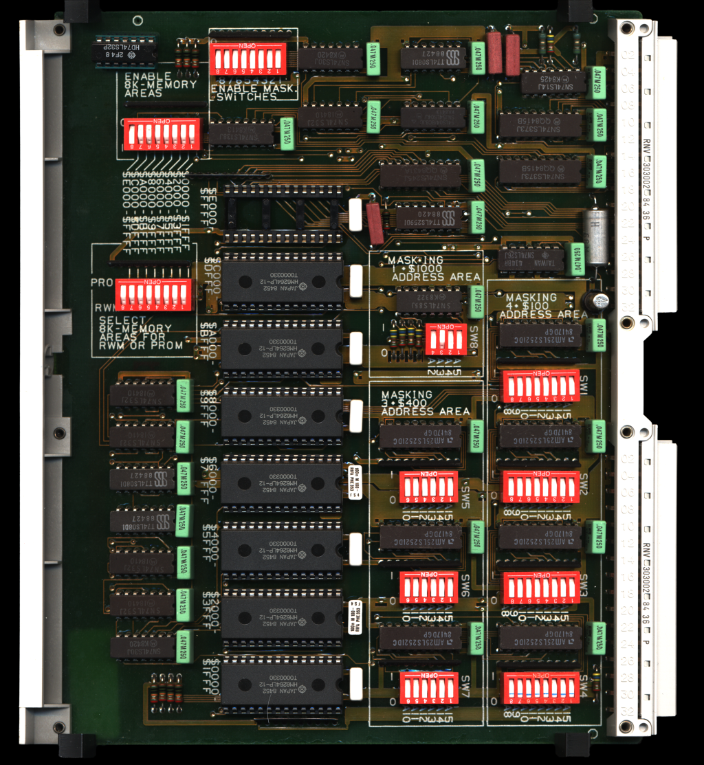
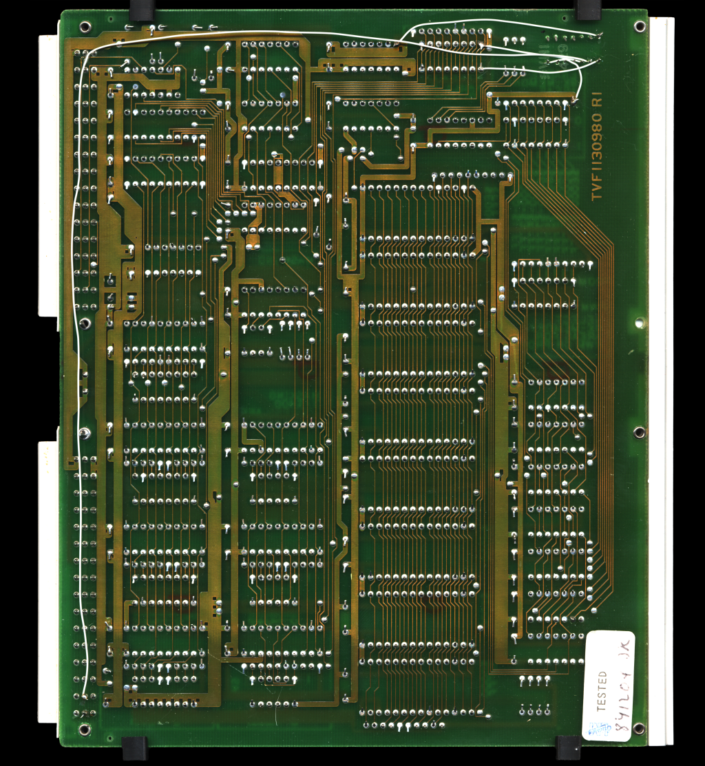
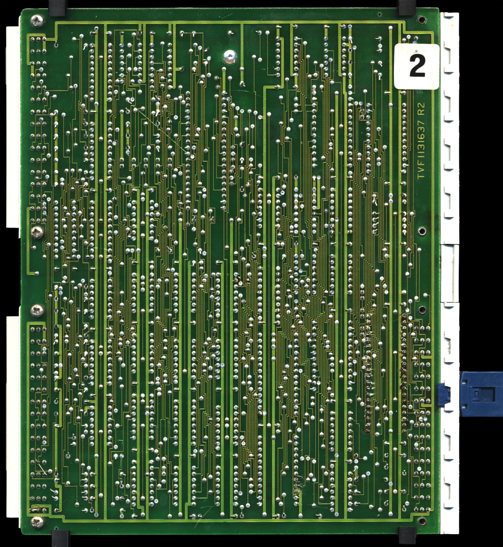
The memory card has room for eight Hitachi HM6264LP-12 static RAMs, each holding 8 kB, giving it a maximum capacity of 64 kB. There's a small catch, though: the scans show seven chips and one empty socket, so this particular card has 56 kB physically fitted. The empty position is labelled $E000–$FFFF. That would make sense as space left for the monitor ROM and I/O, but the actual memory map will have to be checked against the manuals and switch settings.
The HM6264 is SRAM, so there's no DRAM refresh circuitry to deal with, and the -12 parts have a 120 ns access time. Quite a bit of the rest of the board seems to be there to decide when the RAM should not answer. There are switches labelled "ENABLE 8K-MEMORY AREAS" and "SELECT 8K-MEMORY AREAS FOR RWM OR PROM", as well as several groups of address masking switches. The AMD Am25LS2521 chips beside those switches are 8-bit equality comparators, which fits nicely with comparing bus addresses against switch-selected values. A lot of switches for a card whose main job is remembering things :)
There are also two 74LS373 latches, a 74LS245 bus transceiver, and the usual assortment of glue logic. The solder side has a few white bodge wires near one end of the board. Exactly which address ranges are enabled, and what those modifications change, are still things to investigate.
IO card P/N ROF 137 3202
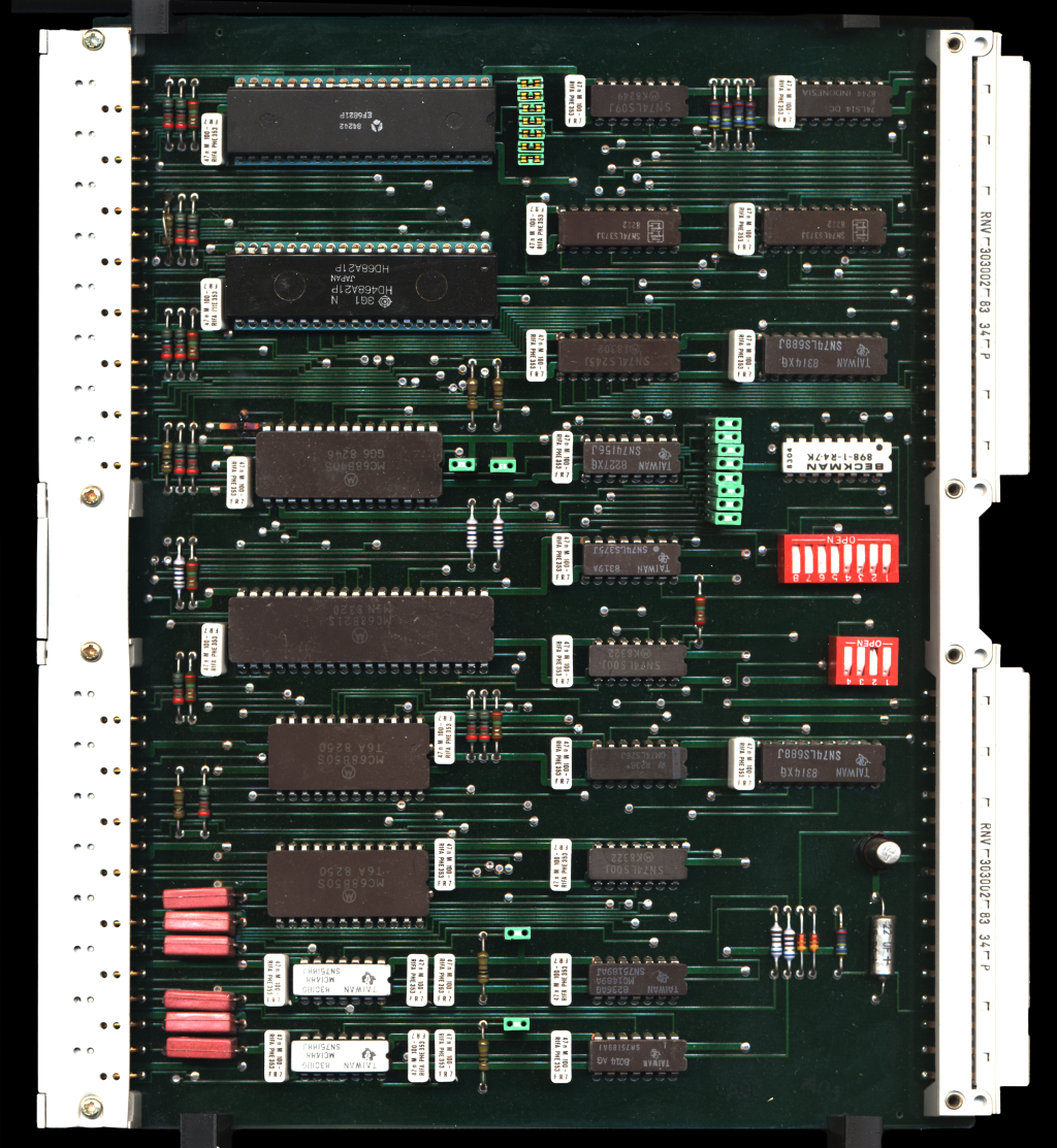
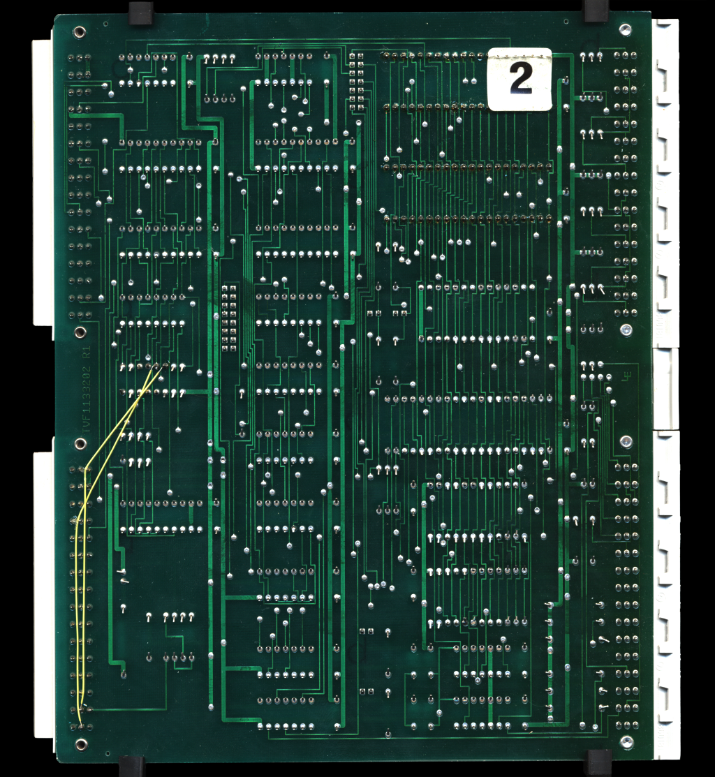
This is where the USE 6800 gets quite a lot of its ability to talk to the outside world. There are two Motorola MC68B50S ACIAs for asynchronous serial communication, and three 6821-family PIAs for parallel I/O: a Motorola MC68B21S, a Hitachi HD468A21P (also marked HD68A21P), and a Thomson EF6821P. A small international gathering of fairly familiar 6800 peripherals.
Each PIA provides two 8-bit ports with programmable data direction, together with control and interrupt lines. That gives the card six parallel ports in total, although it doesn't tell us how they're allocated in this machine. The display/keypad is connected to this card, but which PIA handles which signals will have to wait until the wiring and documentation have been followed a bit further. The two serial interfaces are accompanied by pairs of Texas Instruments SN75188 line drivers and SN75189A line receivers, the parts that handle the electrical side of RS-232. One of the serial channels would be an obvious candidate for the Heathkit terminal, but the connector pinout still needs checking.
There's also a Motorola MC68B40S programmable timer module, with three 16-bit counters, as well as address decoding, latches, a bus transceiver, DIP switches and a collection of jumper positions. Whether the timer is providing serial clocks, general timing, or a bit of both is something I don't want to guess from a photograph. There are two yellow bodge wires on the bottom, so this card has had at least a little attention after the PCB was made.
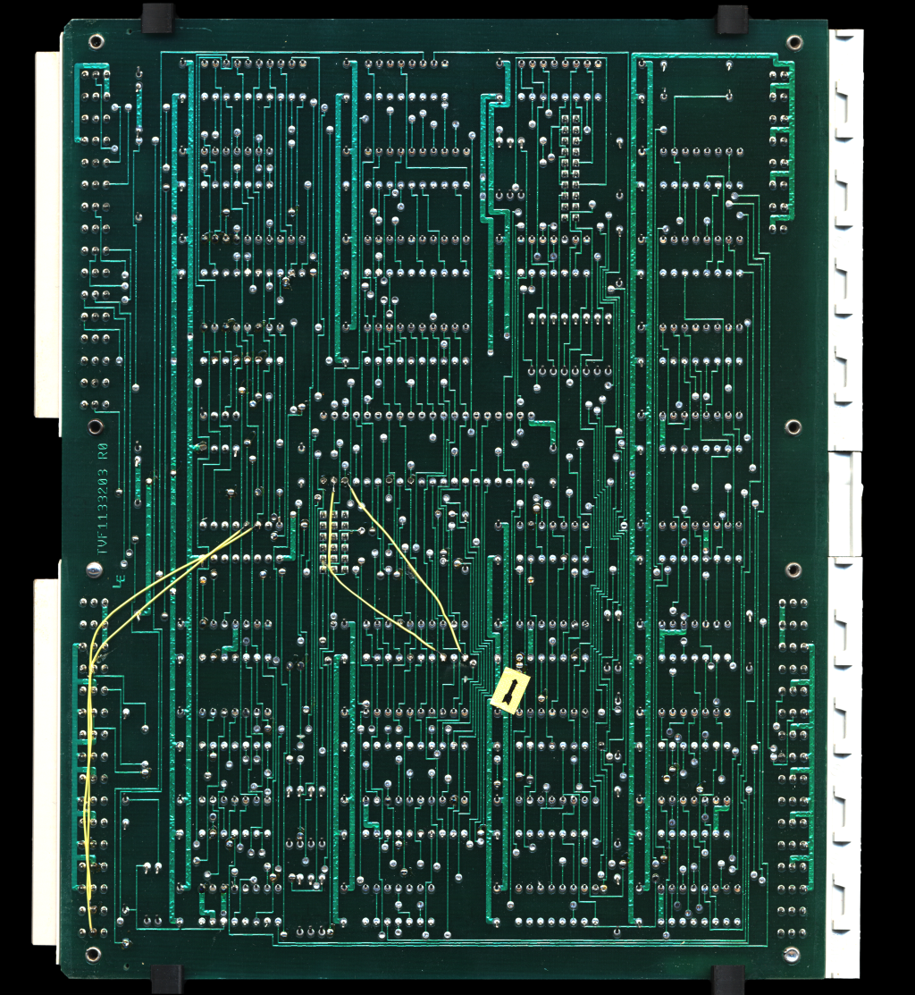
Floppy controller P/N ROF 137 3203
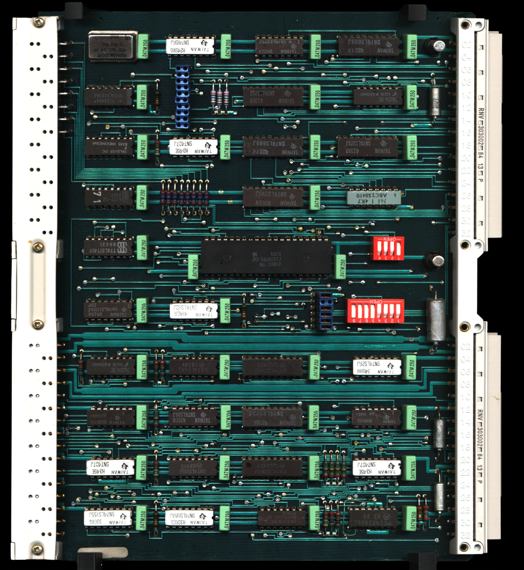
The big IC in the middle is a Western Digital FD1797PL-02 floppy disk formatter/controller. It's part of the FD179X-02 family, with support for both single density FM and double density MFM recording. The 1797 has a non-inverted data bus and a side-select output, which makes it a suitable starting point for controlling double-sided drives. The chip also takes care of things such as stepping the head, finding sectors, and generating and checking CRCs; the CPU doesn't have to interpret every pulse coming off the disk itself.
There's still quite a bit of circuitry around it, though. The board has a Motorola MC14538B dual monostable, a 74LS161 counter, several 74LS373 latches, 74LS688 comparators, a 74LS245 bus transceiver, and plenty of smaller gates and flip-flops. There's also a crystal in a metal can, DIP switches and jumper positions. Identifying the individual parts is one thing; working out exactly how the read-data timing, drive selection and address decoding are implemented will take some tracing. I've saved the Western Digital application notes alongside the datasheet, which should be useful for that.
One particularly interesting little part is the MMI 6331-1J PROM. That's another bit of programmed content worth preserving, even though there's no reason yet to assume it contains boot code. Its actual job will have to be established from the connections and a dump. The underside has several yellow bodge wires, including long runs back to the connector. Given the unusual layout of the floppy I've imaged, I'm quite curious to see how the controller setup and FLEX disk routines fit together. The controller's FM/MFM support alone doesn't establish how that particular disk was recorded.
Power distribution P/N ROF 137 3299
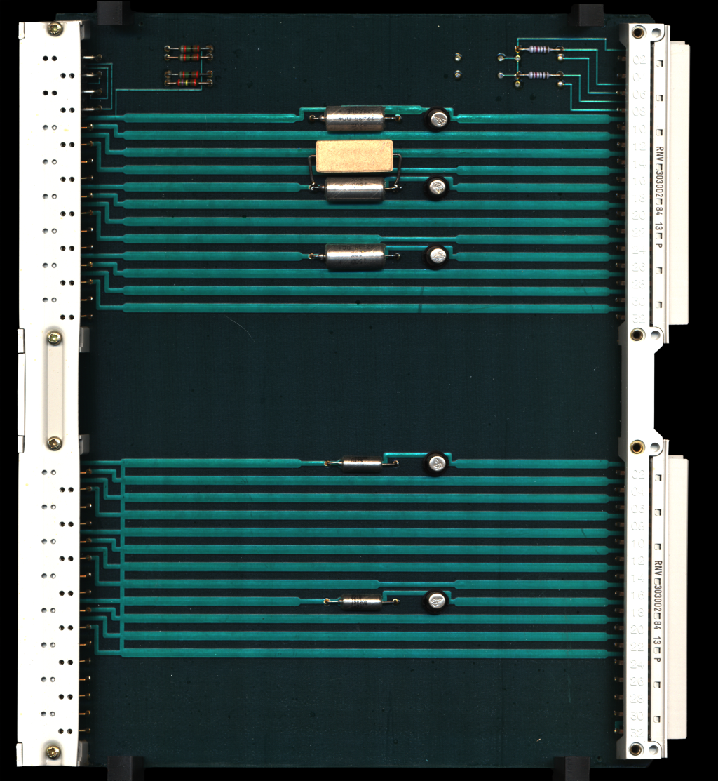
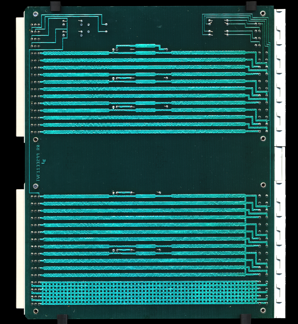
This card is a bit of a change of pace after all the ICs on the other boards. Most of it is wide copper tracks between the two connectors, with a handful of resistors, axial capacitors marked Sprague, and a rectangular encapsulated component. The solder side makes the generous track widths particularly obvious. Apparently even distributing power gets a full-size card in this machine.
There are no obvious regulator ICs or power transistors on it, so it appears to be routing and decoupling supplies rather than producing the supply voltages itself. The exact rails, connector pinout and purpose of the individual passive components still need to be checked; the width of a track doesn't tell us what voltage is on it. This is one of the cards where a continuity meter should get us rather further than a stack of IC datasheets. There are some short wire links, but none of the long bodge wires found on the more complicated boards.
I/O Display/Keypad P/N N/A
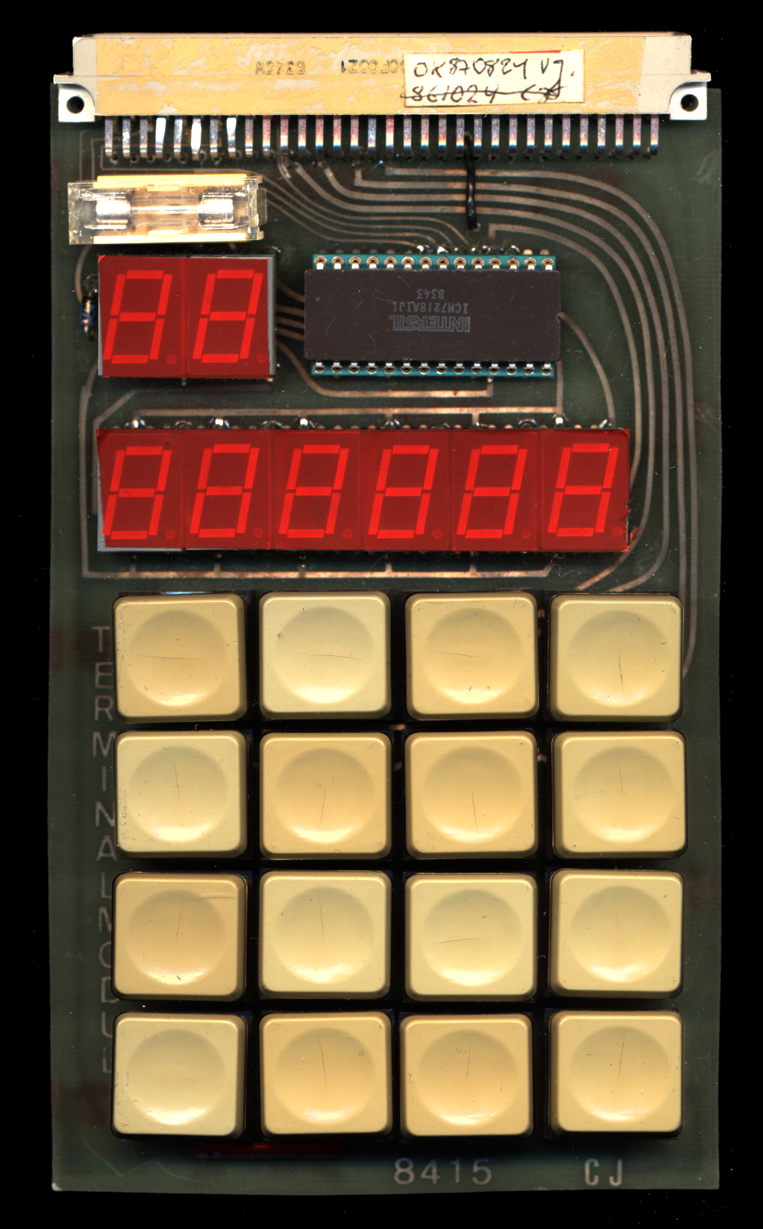

This little board has sixteen keys in a 4×4 arrangement, eight red seven-segment digits (a group of two and a group of six), and an Intersil ICM7218AIJI LED display driver. The driver has its own eight-byte display memory, hexadecimal decoding and multiplexing circuitry, so the computer can write display data and leave the repetitive business of lighting the digits to the chip. The A version is intended for common-anode displays.
The ICM7218 handles the display, but it doesn't scan the keys. The tracks on the underside appear to connect the switches as a row-and-column matrix, with the actual scanning presumably handled through the I/O card. The exact row/column pinout and key assignments still need checking; sixteen keys would make a convenient hexadecimal keypad, but that doesn't establish what the monitor software actually does with them. A display split into two and six digits is equally tempting to assign a meaning to, and I'll resist doing that until there's something in the manuals or ROM to back it up.
There's also a glass cartridge fuse near the connector. Compared with the main cards, the PCB looks much more like a small custom-built peripheral, with broad curved tracks and very little besides the switches, displays and driver. It has "8415" and "CJ" marked along the edge, but no obvious ROF part number in the scans.